PCB DESİGN

PCB Design
Net Elektronik Tasarim firm, with its ongoing design experience for many years, whether it is the realization of a special design or from design to production.
You can meet all your PCB design requests from single-layer to multi-layer, world-class manufacturability and testability.
fully complies with the criteria.
These studies;
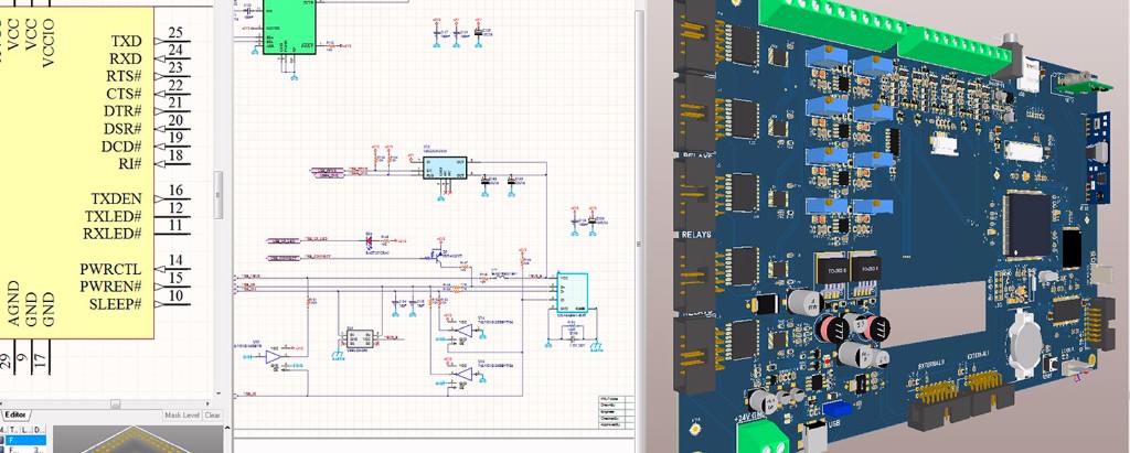
1. Creating/Editing Circuit Diagram
2. PCB layout drawing
3. Mechanical CAD design.
4. It includes Compliance and Verification testing stages.
Creating/Editing Circuit Diagram
Transferring the details of the circuit diagram to the PCB layout is the main issue. Details such as dimensions, technical criteria, and waterway details in the design should be considered.
It is ensured that the PCB layout work is done correctly. Up-to-date information on change requests for products in production is also processed.
The compliance of the PCB layout with the circuit diagram is fulfilled. Different outputs that the production will need are produced and archived.
- Transferring information from different document formats to the schema (Hand drawing, CAD output, etc...)
- Compatibility check of design and schematic files.
- Creating design rules document for each project.
- Transferring the company logo and your unique page structure.
- Creation of data required for printing (PDF, HPGL, DXF or Hard Copy)
- Creation of BOM and parts lists
PCB Layout Drawing
The schematic, circuit diagram designed or provided by the customer will meet the rules and required international standards (IPC)
transferred to the PCB layout in this way. While digital signals are automatically generated by the system; analog, power and some critical electrical values
The paths of the signals are created manually. Single-layer (single - layer) or multi-layer (multi - layer) PCB layout designs are made.
PCB Layout Design Criteria
- analogue, digital
- Multi-level ( 4- 26 +) design
- Compliance with IPC - 2221 / 2 standards
- Manual or automatic waterway routing
- Automatically orientate according to design criteria or component size
- RS - 274D, RS - 274X gerber output
- PCB's technical documents
- Connection diagram and production data in accordance with IPC - 356A standards
Programs Used in PCB Layout Design
Altium Designer
CAM 350
Mechanical CAD design
CAD designs are made in accordance with the PCB layout or in accordance with the customer requests in accordance with IP standards. With the appropriate color and material options, it is possible to work on a wide variety of product groups. The designs created as a result of CAD designs and approved for compliance can be produced with 3D printers or CNC and laser.
Ready-made box designs are recommended for the shell design of the final product.
Compatibility and Validation tests
Mechanical CAD work and PCB layout work are completed and the electrical and functional tests of the produced samples, as well as product verification and compatibility tests are carried out.